

8
2025.12
作者
132
阅读量
With the rapid development of the global electronics industry, the semiconductor industry has expanded significantly, becoming a crucial force driving global technological innovation. Since wafer integrated circuit manufacturing is the core business of this industry, the inspection process for semiconductor chips is particularly important. Silicon, as an excellent semiconductor material, possesses advantages such as abundant resources, low cost, and high stability, making it an ideal choice for chip manufacturing. Utilizing short-wave infrared (SWIR) light, we can achieve spectral imaging with wavelengths greater than 1150nm through silicon wafers. Applying this to the semiconductor chip manufacturing process enables operations such as raw material silicon wafer inspection, grain defect inspection, and edge bonding inspection, thereby significantly reducing manufacturing costs and becoming a powerful and effective inspection tool.
I. Semiconductor Chip Manufacturing Process
Semiconductor device manufacturing is a complex, multi-step process that includes three main stages: wafer fabrication, front-end of line (FEOL, substrate process) and back-end of line (BEOL, interconnect process).
Wafer fabrication refers to the process of purifying polycrystalline silicon from sand in nature, refining it into monocrystalline silicon, and then manufacturing monocrystalline silicon wafers with a purity of up to 99.9999999999% through crystal growth, slicing (using an inside saw or wire saw to cut the ingot into thin slices of about 1 mm thick to form wafers), grinding (the thin slices are polished to the required thickness on a grinding machine with alumina abrasive, while improving surface parallelism), etching (mechanical damage to the wafer surface caused by previous steps can be removed by chemical etching), polishing (the wafer surface is made completely flat and mirror polished using a mechanical and chemical polishing method using colloidal silica), as well as cleaning and inspection.
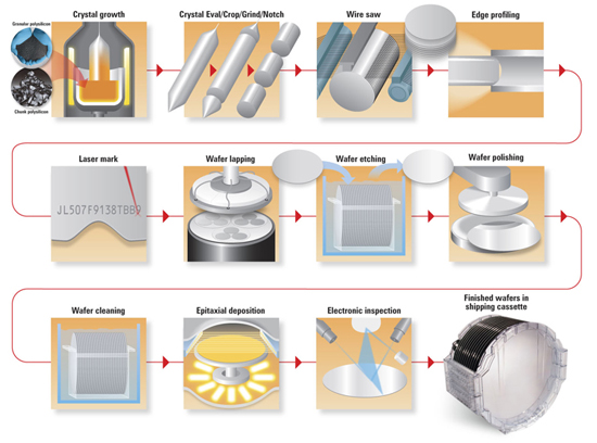
Schematic diagram of wafer fabrication process
The front-end process refers to the process of fabricating device structures on a single-crystal silicon wafer using techniques such as photolithography, doping, and deposition; that is, the process of manufacturing field-effect transistors. See the diagram below for specific steps.

Basic steps of the front-end process: (a) Substrate preparation (b) Oxide mask layer growth (c) Photoresist coating (d) Loading the photomask and aligning it with the wafer (e) Exposure to strong ultraviolet light (f) Removal of excess photoresist with developer (g) Ion implantation to create the source and drain of the transistor.
Once all the components of the IC are ready, the BEOL process is performed, depositing metal wiring between the individual devices to interconnect them. This process is called metallization, as shown in the figure below.

Post-processing steps: (a) Pre-treated wafer (b) Metal deposition (c) Chemical etching to remove exposed portions of the photoresist (d) After etching, obtaining the interconnect wire pattern (e) Various metal layers are interconnected by etching holes (called vias) in the insulating material.
After BEOL processing, post-wafer processes are performed, including wafer testing, die separation, die testing, IC packaging, and final device testing.
II. Application of Shortwave Infrared Cameras
In the above process, infrared cameras are often introduced into testing, inspection and quality control systems, such as: detecting defects such as voids and cracks inside semiconductor wafers, inspecting wafers after stacking wafers, and inspecting chips and packages.
01 Inspection of silicon crystals and ingots
When silicon bricks are processed into wafers, the presence of internal impurities can damage the dicing blades and other production equipment. Using a short-wave infrared (SWIR) camera combined with a specific wavelength light source, impurities and compounds within silicon bricks or ingots can be easily detected, ensuring a safer production process and higher efficiency. This is because the band gap of semiconductor silicon does not absorb lower-energy, longer-wavelength short-wave infrared photons, while higher-energy visible light is absorbed. This makes the SWIR camera an excellent inspection tool, capable of directly detecting impurities, defects, voids, or inclusions.

Silicon ingot testing: Left: Visible light; Right: SWIR.
02 Wafer Bonding Inspection
Multi-stack wafer bonding is one of the most promising fabrication techniques for three-dimensional microstructures. It offers the possibility of independent bonding based on wafer thickness, doping level, crystal orientation, and lattice spacing. Wafer bonding occurs after wafer etching, and the process can be briefly described by the figure below. For the bonding process, a high-quality interface between the contacting wafer surfaces is crucial. Factors such as dust, air, and the integrity of the initial wafer can all contribute to defects in the bonding area. To meet these requirements, the bonding results need to be inspected using an infrared camera to ensure control over its condition at all stages of manufacturing.

Multi-stack bonding steps: (a) the wafer is processed and prepared for bonding; (b) the oxide layer on the non-bonding side is protected with photoresist; (c) the oxide layer on the bonding side is removed by BOE; (d) the wafer is cleaned; (e) and (f) the wafer is annealed at 1050°C and then bonded.
03 Die and Packaging Inspection
Pre-packaging die inspection (i.e., the small pieces into which a wafer is cut) is also a common application of SWIR cameras because they can see small cracks caused by wafer cutting, hidden inside the silicon material (see figure below).

SWIR camera image of grain side view inspection - looking for cutting damage inside silicon
Wafer-level packaging is a technology that combines wafer fabrication and device packaging. Using wafer-level packaging, many integrated circuits can be stacked together through interconnect processes such as TSVs (Through Silicon Vias, a channel for vertical electrical interconnection between three stacked chips, a key element of 3D integrated packaging) or metal stacking, and then packaged. In this process, SWIR cameras are used for seal inspection (detection of bubbles or cracks, see the image below), device defect inspection, critical dimensions, and capping layer measurements.

Shortwave infrared images show sealing failure
04 Photovoltaic wafer inspection
Solar panels are composed of photovoltaic (PV) cells, each of which includes front and rear metal electrodes, a silicon layer, and a textured surface with an anti-reflective coating. Surface scratches, cracks, bubbles, inclusions, and contact forming errors can affect the final efficiency and lifespan of a solar cell. These can be detected using electroluminescence (EL) imaging and photoluminescence (PL) imaging, and can be detected by a SWIR camera.
Electroluminescence is a physical phenomenon in which light is emitted by an electric field generated by a voltage applied to two electrodes. Photovoltaic panels are made of silicon and have an emission peak at 1150 nm. Light emission is directly related to relevant physical quantities (carrier density, diode voltage, etc.). Photoluminescence imaging, on the other hand, uses light excitation. Compared to electroluminescence, its main advantage is that it does not require contact with the sample. In the production process, photoluminescence imaging has great potential as an online monitoring tool for some finished products or finished wafers.
Regardless of the detection method, the emitted signals are all within the short-wave infrared range, requiring a SWIR camera for detection and imaging. From silicon crystals to ingots/bricks, wafers, solar cells, and even solar modules, the application of SWIR cameras can cover the entire supply chain inspection process.

Electroluminescence images obtained using a SWIR camera
SWIR cameras are considered invaluable tools in semiconductor inspection. Their ability to penetrate silicon and other semiconductor materials, along with their high sensitivity and low noise, enables comprehensive defect detection and quality control. Using SWIR imaging equipment, semiconductor manufacturers can effectively increase yield, optimize processes, and improve overall efficiency.